l O GATE Nanosecond Switching Speeds Linear Transfer Characteristics High Input Impedance Description The IRFS40, IRF541, IRF542, and IRF543 are n-channel | Terminal Diagram enhancement-mode silicon-gate power field-effect transis- tors. IRF540R, IRF541R, IRF542R and IRF543R types are N-CHANNEL ENHANCEMENT MODE advanced power MOSFETs designed, tested, and guaranteed to withstand a specified level of energy in the breakdown D avalanche mode of operation. All of these power MOSFETs are designed for applications such as switching regulators, switching converters, motor drivers, relay drivers, and drivers for high-power bipolar switching transistors requiring high G speed and low gate-drive power. These types can be operated directly from integrated circuits. The IRF types are supplied in the JEDEC TO-220AB plastic Ss package. Gi di Zz So <= ec 25 a Absolute Maximum Ratings (To = +25C), Unless Otherwise Specified IRF540 IRF541 (RF542 IRF543 IRFS40R IRF541R IRF542R IRF543R UNITS Drain-Sou
 5 Pages, 193 KB, Scan
>>. GATE Nanosecond Switching Speeds Linear Transfer Characteristics High Input Impedance Description The IRF540, IRF541, IRF542, and IRF543 are n-channel | Terminal Diagram enhancement-mode silicon-gate power field-effect transis- tors. IRF540R, IRF541R, IRF542R and IRF543R types are N-CHANNEL ENHANCEMENT MODE advanced power MOSFETs designed, tested, and guaranteed to withstand a specified level of energy in the breakdown D avalanche mode of operation. All of these power MOSFETs are designed for applications such as switching regulators, switching converters, motor drivers, relay drivers, and drivers for high-power bipolar switching transistors requiring high G speed and low gate-drive power. These types can be operated directly from integrated circuits. The IRF types are supplied in the JEDEC TO-220AB plastic Ss package. a du 2M zo <= cae z a Absolute Maximum Ratings (Tc = +25C), Unless Otherwise Specified IRF540 IRFS41 IRF542 IRFS43 IRF540R IRFS41R IRF542R IRF543R UNITS Drain-Sour
 5 Pages, 398 KB, Scan
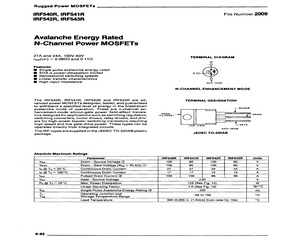
IRF542R, IRF543R Avalanche Energy Rated N-Channel Power MOSFETs 27A and 24A, 100V-60V fos(on) = 0.085Q and 0.110 Features: BH Single pulse avalanche energy rated @ SOA is power-dissipation limited lM Nanosecond switching speeds @ Linear transfer characteristics Hf High input impedance The IRF540R, IRF541R, IRF542R and IRF543R are ad- vanced power MOSFETs designed, tested, and guaranteed to withstand a specified level of energy in the breakdown File Number 2009 TERMINAL DIAGRAM 0 9208-42658 N-CHANNEL ENHANCEMENT MODE TERMINAL DESIGNATION avalanche mode of operation. These are n-channel en- cS SOURCE hancement-mode silicon-gate power field-effect transis- pRAIN ! tors designed for applications such as switching regulators, (FLANGE) -______ DRAIN switching converters, motor drivers, relay drivers, and driv- OC ers for high-power bipolar switching transistors requiring = => high speed and low gate-drive power. These types can be GATE operated directly from integrated circuits. TOP VIEW 9
 5 Pages, 194 KB, Scan
 Voo = 25V, Start Ty = +25C, L = 9.2mH, 2. Pulse Test: Pulse width < 300us, junction temperature. See Transient Thermal Res = 252, IpEAK = 13A (See Figure 15) Duty Cycle < 2% Impedance Curve (Figure 5} 4-267IRF450, IRF451, IRF542, IRF453 IRF450R, IRF451R, IRF542R, IRF453R Performance Curves 20 102 1 PULSE Vpg 2 50V SE TEST gq 16 a @ w by 10 ac wu g a 5 : z 12 = 5 5 wu us C vd 1 g 3 es) a oO qi z < a 2 5 z 90.4 eos os 4a.5V 2 72 50 100 150-200 roo 2 4 6 8 10 Vpg- ORAIN-TO-SOURCE VOLTAGE (VOLTS) Vgg. GATE-TO-SOURCE VOLTAGE (VOLTS FIGURE 1. TYPICAL OUTPUT CHARACTERISTICS FIGURE 2. TYPICAL TRANSFER CHARACTERISTICS IN THI Fos (ON) Ip. DRAIN CURRENT (AMPERES) Ip. ORAIN CURRENT (AMPERES) Tex25C IRF a5 Ty=150C IAF : 0.4 INGLE PULSE Qo 3 6 9 42 15 42 5 40 2 5 492 2 5 403 Vog: DRAIN-TO-SOURCE VOLTAGE (VOLTS) Vps: ORAIN-TO-SQURCE VOLTAGE {VOLTS FIGURE 3. TYPICAL SATURATION CHARACTERISTICS FIGURE 4, MAXIMUM SAFE OPERATING AREA , 10 Q a] x= Sy W no S mS ne 0.4 Pom a) w wt ; ety 310 jt ed 4 NOTES: = 1. DUTY FA
 5 Pages, 194 KB, Scan


